Printed circuit boards (PCBs) are manufactured for soldering and solder removal done by professionals. Newer DIY builders, particularly when troubleshooting an issue, can easily damage PCBs. Having a trace lift or pad crumble off your PCB may seem catastrophic, but it's really not a big deal and is easily fixable.
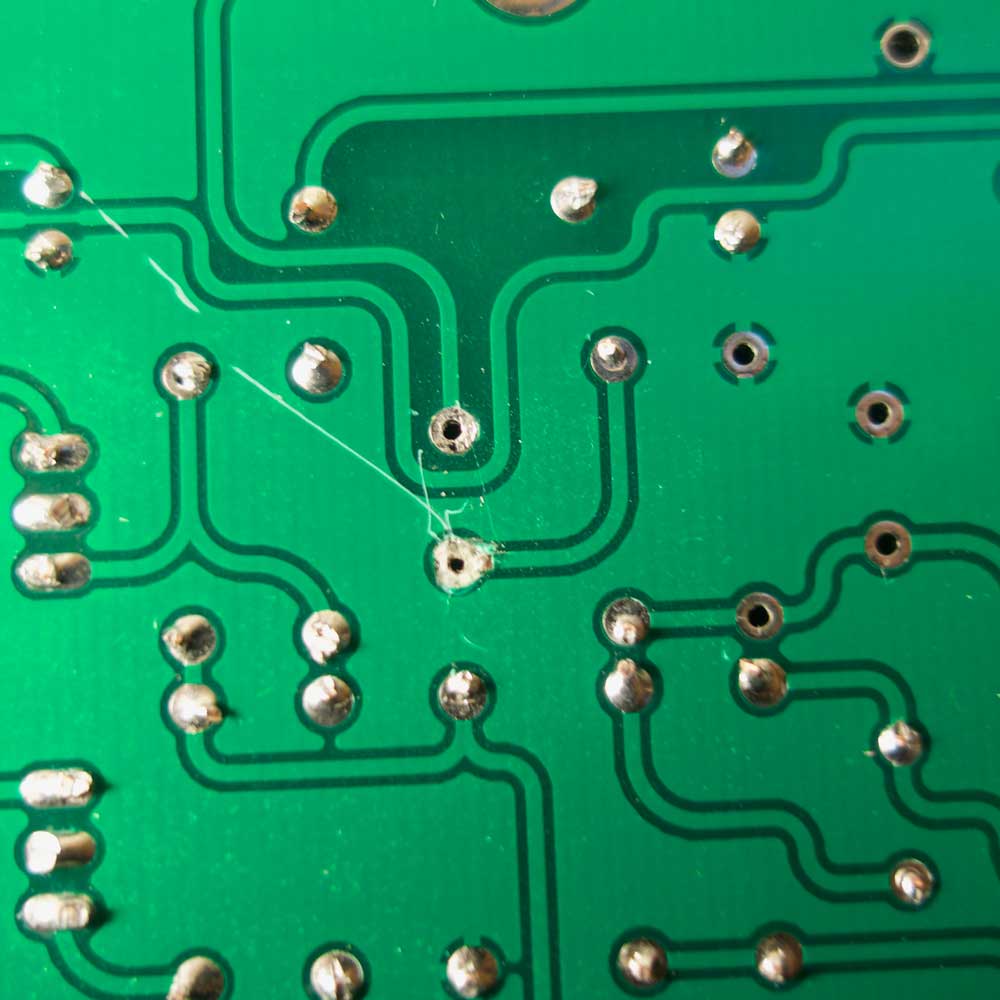
In the example below, you can see a pad has been burned off the PCB from excessive heat and pressure on the pad. What remains is the PCB material, called FR-4. It's a non-conductive mix of woven glass and epoxy. Obviously, you can't solder a component to it.

In this case you can see the trace connected to the pad location. It's a singular trace the leaves the right side of the pad and travels up to another pad. This connection can be confirmed by checking the schematic.
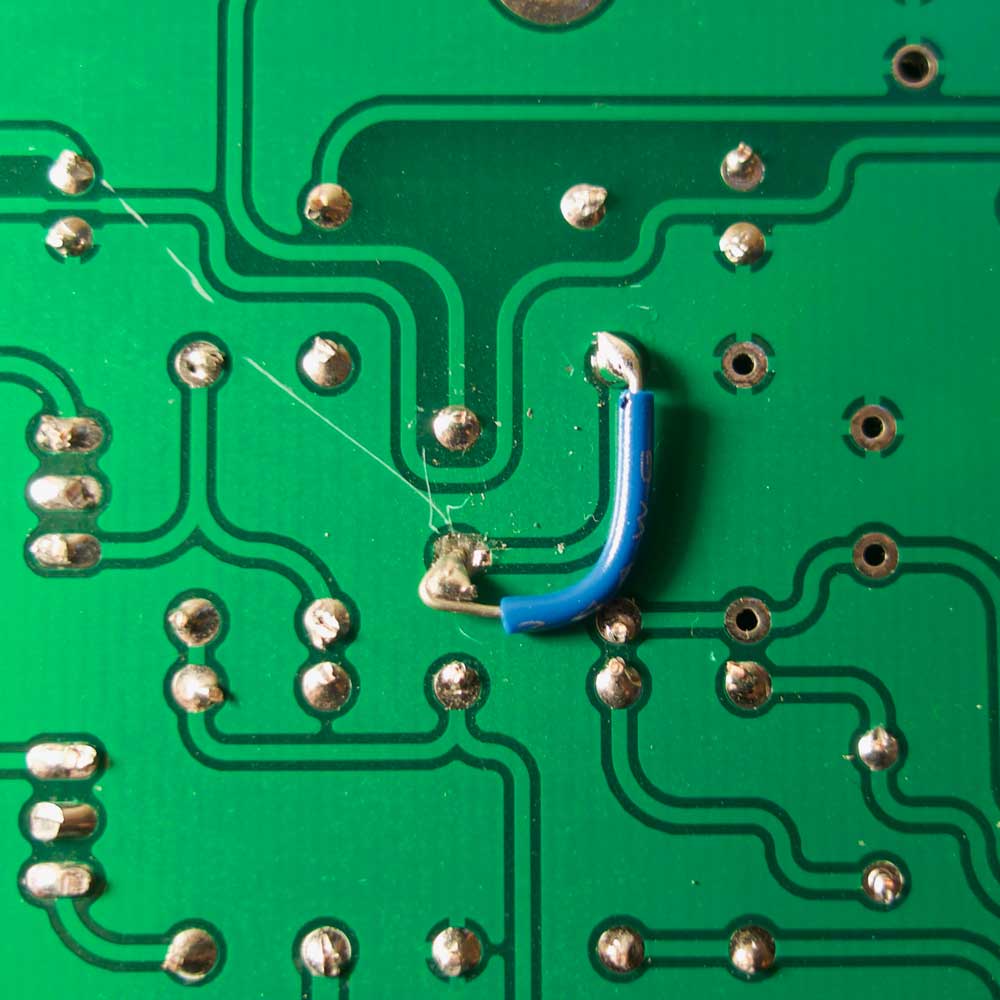
To fix it, simply use a short wire to reconnect the two leads. Solid core wire works best but whatever you have should work. In this case, I've connected a signal trace using 22ga solid core wire by soldering it to the two connected component leads.

It's important to inspect both the top and bottom side of the PCB pad. If the pad is damaged on both sides of the PCB, you'll need to check for traces on the top and bottom. If the pad is not damaged on both sides or there are only traces on one side, you only need to repair the damaged side or may not have to make a repair at all. You should also consider the thickness of your trace, particularity with larger supply lines. If the trace is much larger and thicker, you might want to consider a larger gauge of wire like a 16ga.
Another issue you may encounter is an issue with a ground pad. Ground pads are easily identifiable by their crossed thermal relief pad.
The PCB above has several ground pads, including those in the red box. These ground pads are connected to the ground plane. The ground plane is a large area of copper covering an entire side of the PCB. If the pad was 100% connected to the plane, it would be impossible to get a good solder joint. The plane would act as a giant heatsink to the solder tip. For this reason, the pad makes smaller connections to the plane through thermal relief tracks. Should you damage one of these pads, you can connect the component lead to another ground pad on the PCB. Look for the closest ground pad and confirm with your DMM Ω setting it's connected to the ground plane of your PCB. Make the connection with a short wire and your component lead will be reconnected to the ground plane.
No matter how extensive the damage may seem, if you carefully consider what connections may have been broken, pads and traces are easily fixable. Taking a deep breath and a few minutes of inspection can save many hours and the cost of starting over.

